
sales@brightlx.com

Views: 0 Author: Site Editor Publish Time: 2026-10-14 Origin: Site


What is a stencil?
A stencil is a thin metal foil with laser-cut openings. It is placed over the PCB pads, and solder paste is printed through those openings. The stencil acts like a mold: it controls exactly how much paste lands on each pad. If the paste does not release cleanly, defects follow—bridging, insufficient solder, tombstoning, and solder balls.
How paste transfer works
Solder paste sticks to two things: the PCB pad and the stencil walls. For a good print, the paste must prefer the pad. If the aperture is too small or too deep, paste clings to the stencil instead of transferring. That is why stencil geometry matters more than most engineers expect.
Two numbers predict whether paste will release:
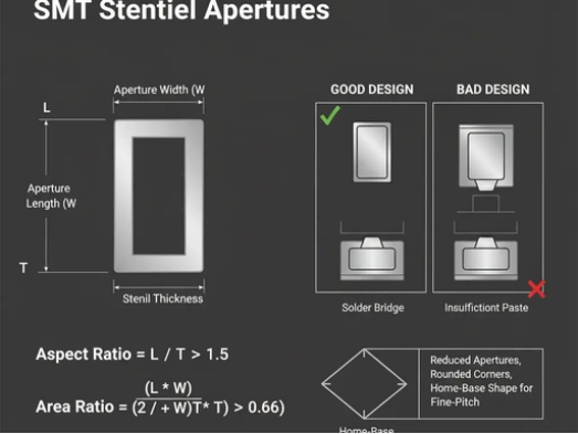
Aspect Ratio (W/T) = aperture width ÷ stencil thickness. IPC-7525 requires ≥1.5.
Area Ratio (L×W) / [2×(L+W)×T] = aperture opening area ÷ aperture wall area. The industry floor is 0.66.
Below these limits, paste sticks to the aperture walls. You get incomplete deposits and random volume—no reflow profile can fix that.
Stencil thickness sets paste volume. Start with the finest-pitch part, not the largest.
If a board mixes fine-pitch ICs with large connectors, use a step stencil: thinner in fine-pitch areas, thicker where more paste is needed.
Component | Recommended Thickness |
0201 / 01005 | 0.06–0.08 mm |
0402, 0.4 mm BGA | 0.08–0.10 mm |
0.5 mm QFP/BGA | 0.10 mm |
0603/0805 | 0.12–0.15 mm |
For 0.5 mm pitch QFP, reduce aperture width to 50–75% of pad width and use a home-plate shape to prevent bridging.
For QFN thermal pads, use a windowpane grid covering 50–80% of the pad. A solid deposit can cause floating and voiding.
Laser cutting is standard and accurate to about ±10 μm, but the walls can be rough. Electropolishing smooths them. Nano-coating can raise paste transfer efficiency by 15–25% for 0.4 mm BGA and below.
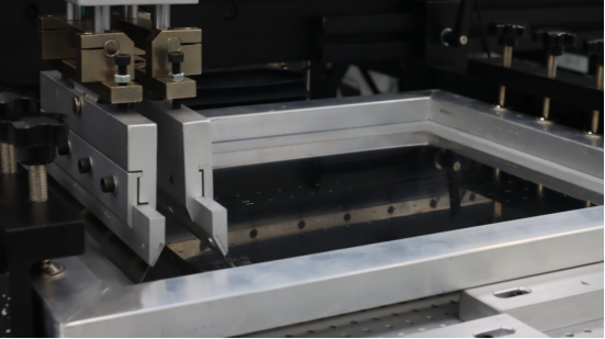
As a PCBA factory with our own SMT lines, we source stencils from trusted partners and also accept custom PCB orders. Our fully automatic solder paste printer supports stencils up to 1500 mm × 500 mm with ±0.025 mm accuracy. Cycle time is under 7 seconds per board, and changeover takes less than 5 minutes—good for high-mix, low-volume orders. We support 0402 components and 0.4 mm fine-pitch ICs, and work with precision PCBs, LED, automotive electronics, and medical boards. Whatever board size you have, we can handle the printing side.
Conclusion
A stencil is not just a "metal sheet with holes." It controls how much paste reaches each pad and directly affects bridging, insufficient solder, tombstoning, and solder balls. Aspect ratio, area ratio, thickness, aperture shape, and surface treatment all matter.
At BRIGHTLX, we understand these details. We source stencils from trusted partners, print with a printer up to 1500 × 500 mm at ±0.025 mm accuracy, and store them vertically after cleaning—no stacking, no deformation. From stencil selection to print parameters, we keep it under control to ensure your PCBs meet the highest quality standards. Contact us today to discuss your assembly needs.


